ABOUT US
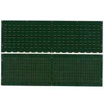
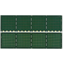
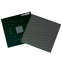
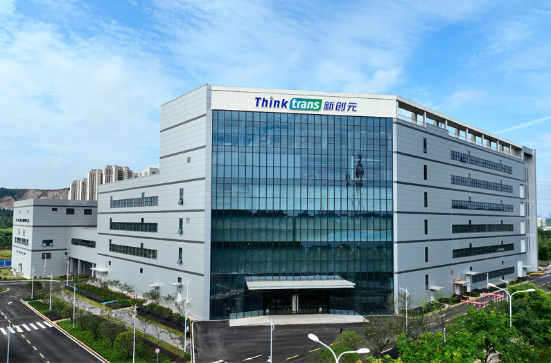
Thinktrans Semiconductor Technology Ltd. was established in 2021 through the restructuring of Thinktrans Optics Valley and Thinktrans Zhuhai. The company headquarters is located in Jiu Long Lake Street, Optics Valley Future Science & Technology City, Wuhan, covering an area of about 150 acres. With a projected total investment of 6 billion yuan, its primary product is the packaging substrate in integrated circuits. The company possesses original core technologies, such as ion-implanted plating, which allows for the creation of circuits with finer lines than conventional processes. The company's customers and products primarily target the following sectors: CSP substrates based on BT materials for memory chips, mobile phones, and primary ICs for TVs; FC-BGA substrates based on···

CORE TECHNOLOGY





Ion Implantation Vapor Deposition
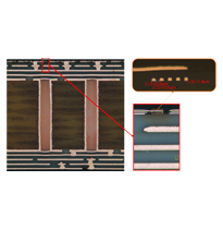
Ion Implantation Vapor Deposition: This unique technology developed by Thinktrans achieves metallization of the substrate surface by injecting metal ions. Unlike traditional chemical copper plating te detail
IVD SAP
Ion Implantation Semi-Additive Process (IVD SAP): Based on the IVD technology, this process improves and enhances the existing SAP process. Unlike traditional semi-additive processes, I-SAP has advant detail
Quick Navigation
Contact Us(Wuhan)
TEL:027-59403688
Address: Thinktrans Factory, Jiulonghu Street, Future Road, East Lake High-tech Development Zone, Wuhan
Email: sales@thinktrans.cn
Contact Us(Shenzhen)
TEL:0755-36516066
Address: South Gate 1,No 20, Songtang Road,Tongfuyu Industrial Park,Tangxiayong,Yanluo Bao'an,Shenzhen,Guangdong, China
Email: sales@thinktrans.cn


